Laser photolithography & UV exposure :
Microelectronics
Microelectronics: direct laser writing and mask alignment for semiconductor manufacturing


Micro-technologies were initially developed to answer the needs of microelectronics and its evolution.
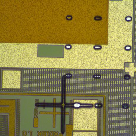
Essentially based on a thin-layers technology (often less than one micrometer), on semiconductor materials, the microelectronics functions have been more and more miniaturized for more than 30 years, to allow the manufacturing of electronics components increasingly miniaturized. Presently, the size of smallest patterns are now lower than 32nm.
Specific needs of microelectronics technology
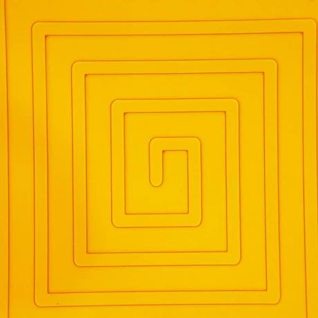
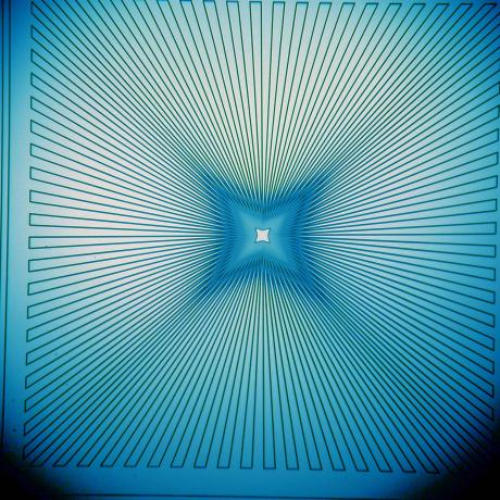
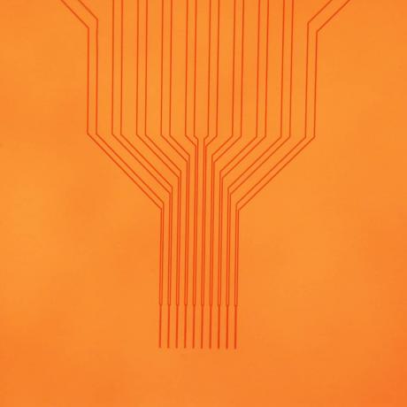
For mutualization reasons of the manufacturing stages, the masking techniques hold an important place. However, the manufacture of photomasks continues to be done, according to resolutions wanted, either by laser writing (down to 500nm) or by electron beam lithography (below to 500nm linewidth).
Some complex functions can have up to 15 or even 20 successive masking levels with increasing pattern densities and resolutions ever finer, for example for microprocessor manufacturing.
Masking, and thus the manufacture of very high resolution photomasks, remains a key point for this activity. Since the thicknesses of resins used are extremely low (<1μm), no specific beam shaping is required apart from, of course, the focusing of the beam.
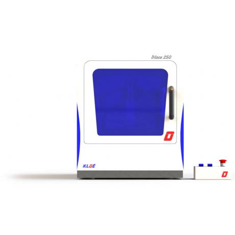
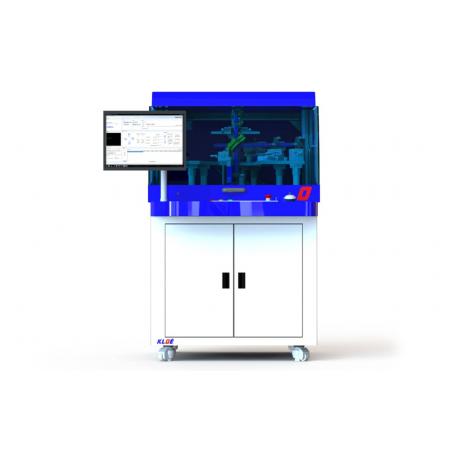
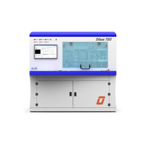
The direct laser writing equipment, Dilase range by Kloe, meet these specifications and enable the manufacture of high quality photolithography masks
Our laser lithography systems offers to the user a necessary flexibility to write directly with a laser on all dimensions wafers as well as on very small samples, with no size limit nor loss of resolution.
The Dilase technology is ideal if you plan to do rapid prototyping directly on wafer or samples with various thicknesses and/or small dimensions. Our laser writers offer the user a much larger flexibility which is essential for the development of new functions on any tape of substrate and for any type of application.
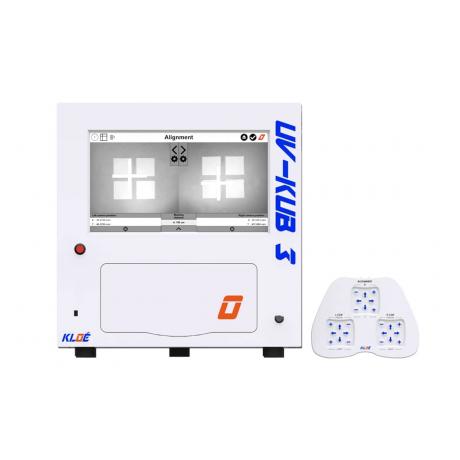
Moreover, Kloe developed the new generation of mask aligners, UV-KUB 3, now available in 6 inches version, perfectly suited for semiconductor manufacturing
This equipment incorporates all the latest technological innovations, such as:
- a UV LED based source perfectly monochromatic, at 365nm, with no infrared emissions
- a flat touch screen
- CCD cameras (instead of binoculars)
- a control joypad
- an embedded PC to register alignment mark and ensure an automatic prealignment.
Compact, fast and safe, the mask aligner UV-KUB 3 is also financially accessible to the larger possible number.