Laser photolithography & UV exposure :
Surface functionalization
Surface functionalization: the importance of the large depth of focus


Surface functionalization, also known as surface structuring, is the ability to modify or adapt the physico-chemical properties of a material.
Microtechnologies are also used increasingly for surface functionalization, to give a surface or an object different or accumulated physico-chemical properties like hydrophobic or hydrophilic properties or acoustic or optical properties.
Specific needs of surface functionalization
The surface functionalization requires nowadays more and more resolution: the machining methods, by mechanical etching or laser, are no more enough precise...
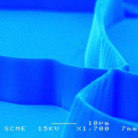
Laser photolithography offers a new perspective by gaining up to an order of magnitude when compared to conventional technologies and thus enabling to achieve high aspect ratio micro and nanostructures.
With direct laser writing technology, it is possible to modify the properties of a surface by simple lithography of a layer or even directly of the surface itself.
A surface can thus become hydrophobic by making a matrix of high aspect ratio micropillars (1x20, 1x50 and even higher), or hydrophilic by modifying the adhesion properties of the surface.
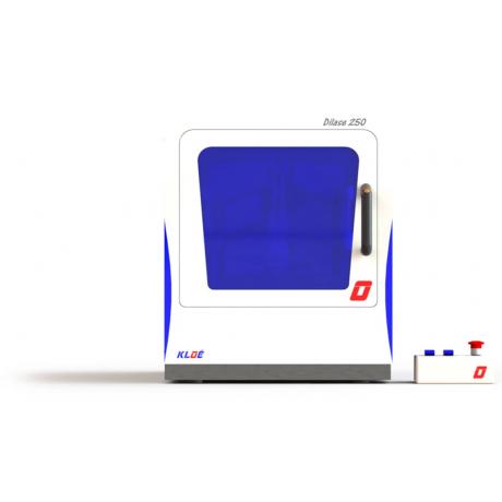
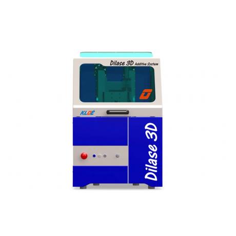
A multitude of surface functions can thus be obtained thanks to high aspect ratio structures, which constitutes one of the specificities of our direct laser writing equipment, Dilase range. These systems are indeed equipped with a suitable laser beam shaping exhibiting very large depth of focus.
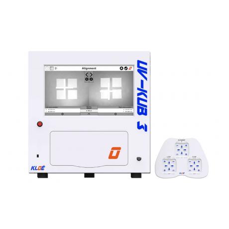
Another way to realize surface functionalization is using our UV-LED masker UV-KUB 2 or our mask aligner UV-KUB 3 by an innovative approach of photolithography.
By manufacturing microstructures with masking lithography, it is thus possible to realize surface structuration, with an aspect ratio of 1x10 by simple masking process.