Laser photolithography & UV exposure :
Photonics
Optics & Photonics: the essential role of vectorial mode in maskless lithography


Photonics is to optics what microelectronics is to electricity.
The basic functions of photonics are:
- the optical waveguide
- the Bragg grating.
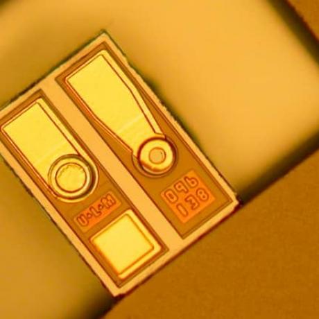
These functions must be realised with extreme precision and must not have any structural defects over some tens of nanometres, because they are destined to transport electro-magnetic waves of a few hundred nanometres wavelengths.
Specific needs of Photonics and Optics technology
The main specifications required to produce integrated optical functions are :
- Resolution and homogeneity over large areas,
- Extreme finesse of the edges of written microstructures
- Low roughness
- The ability to materialize greyscale structures with a very low roughness of the order of ten nanometers.
A waveguide which the roughness would be some hundred nanometres can only guide the light on a few hundreds of microns before the power is dispersed out from the waveguide. Making waveguides with raster scan based writing technique is as a result not possible. It is therefore necessary to have a real vector writing mode.
Furthermore, these integrated optical functions must generally be coupled to optical fibers, where the inner diameter is a minimum of 8µm.
To limit the coupling losses between the waveguides and the optical fibers, the inner dimensions of the waveguides must be of equal diameter. The production process must therefore offer a sufficient depth of focus to manufacture controlled structures on the whole thickness of the layer, namely about ten microns minimum.
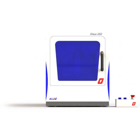
The Dilase technology, direct laser writing range, has been originally developed for the manufacture of integrated optical circuits dedicated to the telecoms and optical sensor markets
As a result, our equipment is naturally and implicitly addressed to this scientific and industrial community. As an example of active collaboration in this sector, Kloe worked for more than 10 years with and for Essilor International.
Kloe initially developed the vector write mode for the fabrication of optical waveguides, because writing by a raster scan technique intrinsically induces too much roughness incompatible with light guidance without excessive propagation losses.
Our direct laser equipment range is equipped with very high resolution writing heads with a large depth of field. This ensures high stability and homogeneity of the linewidth along all trajectories.
Finally, thanks to the vector write mode and the great depth of field, the user of Dilase laser lithography technology benefits from an unlimited number of gray levels simply by modulating, in real time, the writing velocity and the laser power.
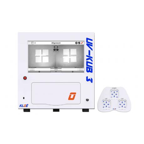
The UV-LED masker UV-KUB 2 and mask aligner UV-KUB 3 are particularly suited for the creation of integrated optical circuits thanks to their unrivalled collimation performance:
- That enables the achievement of microstructures with less than 1µm of resolution
- That guaranteed edges with excellent verticality and no excessive roughness, as well as in thin layers than in thick layers
Thanks to the large depth of focus, it is now possible to proceed thick resist layers with quasi vertical sidewalls.