Laser photolithography & UV exposure :
Greyscale levels
Greyscale levels, microlens and blazed gratings:direct laser writing application


Nowadays, micro-technologies are not reserved exclusively to semiconductor and microelectronics applications.
Many other domains call for micro-technologies to manufacture micro-elements, such as high aspect ratio or greyscale, microlens and blazed gratings. In lithography, we use to call “greyscale applications” those, which refer to partial polymerization of the overall photoresist thickness.The greyscale applications could be use for the manufacturing of microlens, optical circuits, MEMS, blazed gratings…
Specific needs of greyscale levels, microlens and gratings
To realize a greyscale application, it is necessary to modulate the dose (which results in the power density by the resin for the duration of the exposure). Naturally, the thicker the layer, the more the contrast and the number of levels will be visible and necessary.
However, the quality of the final function produced will depend on the capacity to discriminate different grey levels in a linear manner (micro-lens or blazed gratings) or on the contrary in an abrupt way (index or phase contrast function, Fresnel lens).
It is therefore essential that the technology used is compatible with the writing in thick layers as well as thin layers and that the number of grey levels (number of possible dose) is not limited.
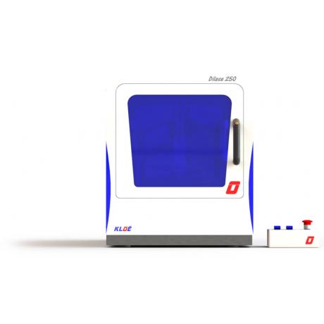
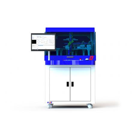
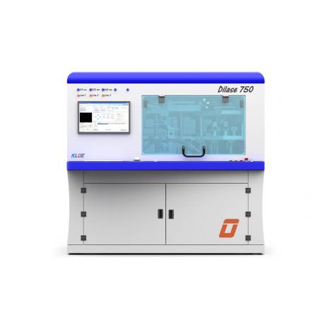
The technology developed by Kloe with its direct laser writing equipment is thus perfectly adapted.
Indeed, it associates large depth of the focus (compatibility with the writing of thick layers with the same rendering as in thin layers without modifying the focusing distance), the vector write mode and the modulation in real time of the writing speed and the emission power of the laser.
Consequently, the number of grey levels is unlimited, varies in a controlled and continuous manner in photoresist thicknesses ranging from a few nanometres to a hundred of microns.